
系统工程与电子技术 ›› 2025, Vol. 47 ›› Issue (4): 1184-1194.doi: 10.12305/j.issn.1001-506X.2025.04.15
关旗龙1, 杭春进1,2,*, 李胜利1, 唐晓玖1, 于丹3, 丁颖3
收稿日期:2023-11-07
出版日期:2025-04-25
发布日期:2025-05-28
通讯作者:
杭春进
作者简介:关旗龙 (2000—), 男, 博士研究生, 主要研究方向为电离辐照环境下Sn基钎料焊点可靠性、Sn基钎料焊点氧化行为第一性原理计算Qilong GUAN1, Chunjin HANG1,2,*, Shengli LI1, Xiaojiu TANG1, Dan YU3, Ying DING3
Received:2023-11-07
Online:2025-04-25
Published:2025-05-28
Contact:
Chunjin HANG
摘要:
深空环境(深冷、极高温和强辐射等)严重影响星载器件的性能及可靠性, 影响深空探测航天器安全运行。锗硅(SiGe)器件主要适用于低温和强辐射环境, 碳化硅(SiC)和氮化镓(GaN)半导体是适用于所有极端环境的理想器件。极高温环境下, 器件封装材料服役可靠性成为星载半导体器件进一步发展的巨大挑战。梳理国内外关于硅(Si)、绝缘体上硅(SOI)、SiGe、GaN和SiC器件以及器件封装材料在上述极端环境下的可靠性研究。针对上述半导体器件和封装材料的特点做出了服役环境总结以及使用建议。
中图分类号:
关旗龙, 杭春进, 李胜利, 唐晓玖, 于丹, 丁颖. 深空环境下电子器件可靠性研究进展[J]. 系统工程与电子技术, 2025, 47(4): 1184-1194.
Qilong GUAN, Chunjin HANG, Shengli LI, Xiaojiu TANG, Dan YU, Ying DING. Review on reliability of electronic devices in deep space environment[J]. Systems Engineering and Electronics, 2025, 47(4): 1184-1194.
表1
太阳系近地星球表面温度"
| 星球 | 环境温度/℃ | 星球 | 环境温度/℃ | |
| 月球 | -180~160 | 水星 | -173~427 | |
| 金星 | 464 | 木星 | -108 | |
| 土星 | -139 | 天王星 | -224 | |
| 海王星 | -218 | 火星 | -133~27 |
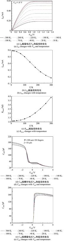
图1
SOIn型MOSFET器件参数随温度的变化"
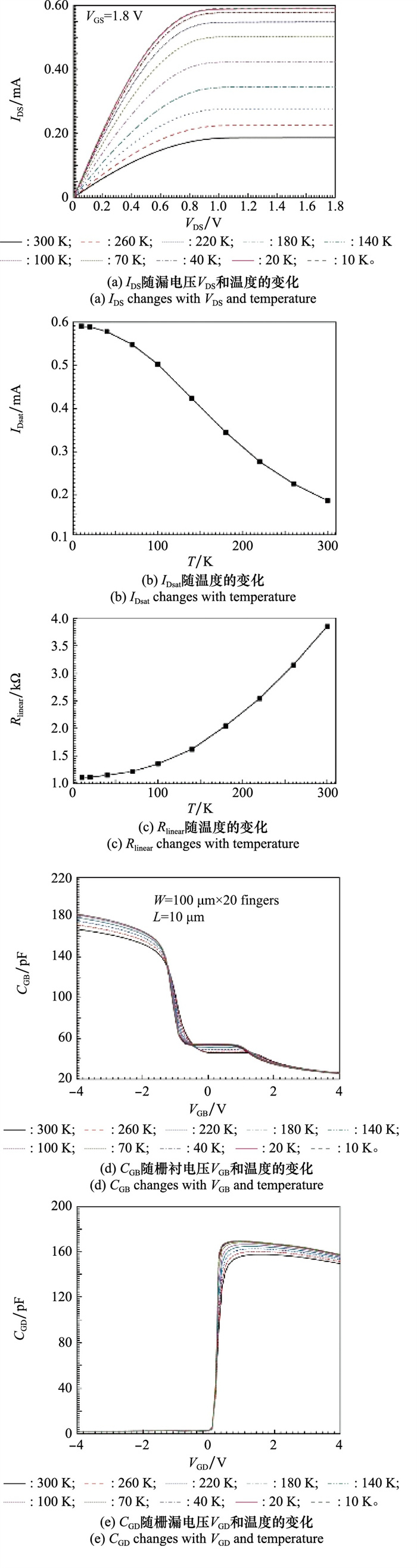

图2
0.12×10.0 μm2 SiGe HBT器件电流增益、截止频率、最大振荡频率、最小噪声系数与偏置电流和温度的函数图"
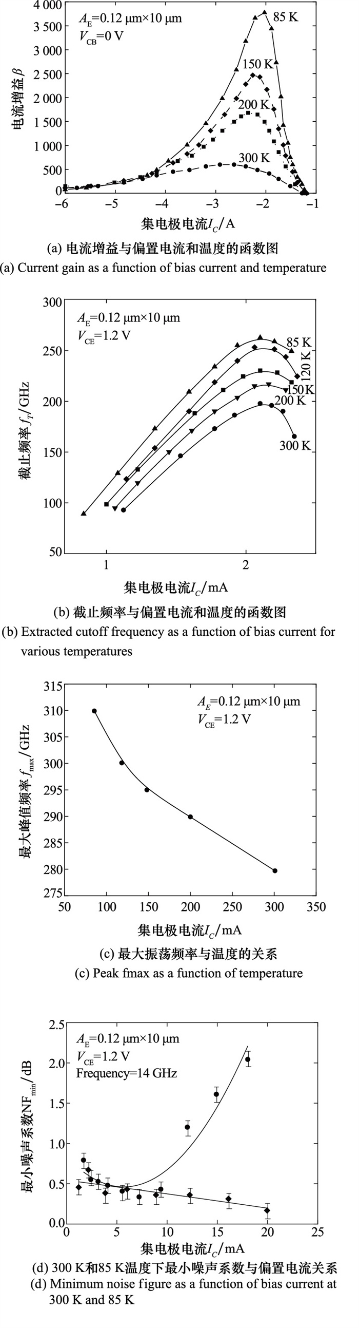
图3
半导体本征载流子浓度与温度的关系"

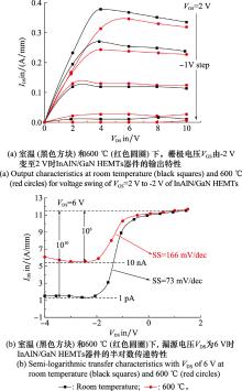
图4
室温和600 ℃下, InAlN/GaN HEMT器件的IDS-VDS和IDS-VGS图"
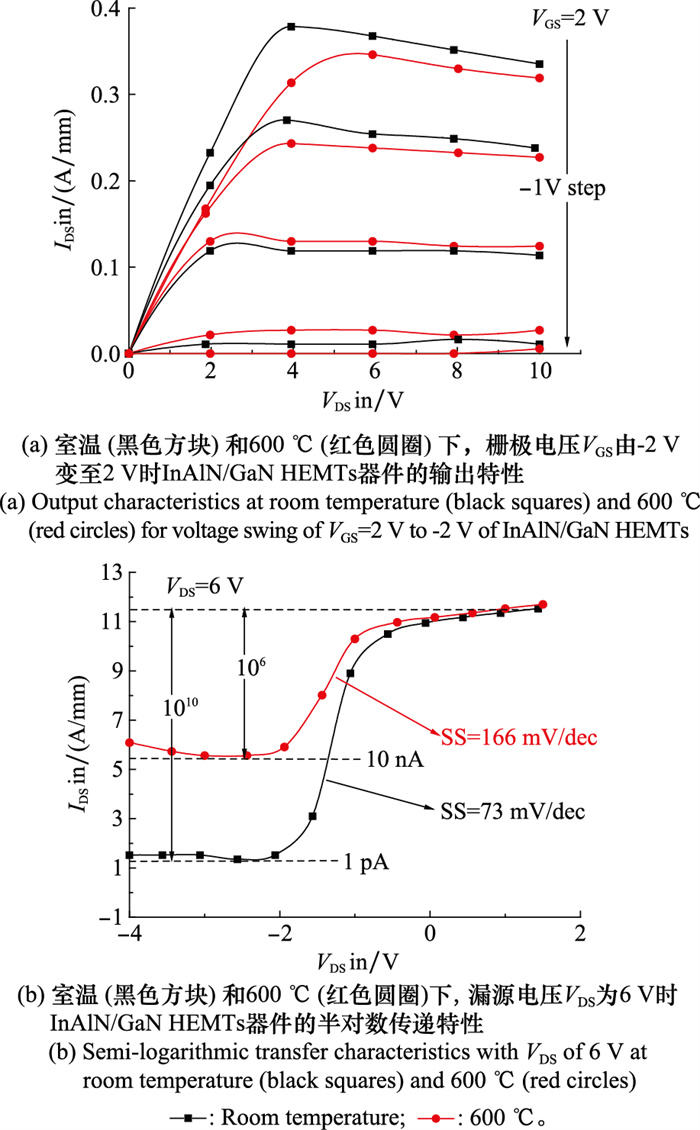
图5
SiC MOSFET器件阈值电压和导通电阻随温度的变化"
表2
深空环境下不同类型电子器件的性能比较"
| 器件类型 | 深空环境下电子器件性能 | |||
| 低温 | 高温 | 辐射 | ||
| Si | 良 | 差 | 差 | |
| SOI | 良 | 良 | 优 | |
| SiGe | 优 | 良 | 优 | |
| SiC | 良 | 优 | 优 | |
| GaN | 优 | 优 | 优 | |
表3
不同金属引线-金属焊盘键合的温度限制"
| 金属引线- 焊盘 | 最高工作温度/℃ | 缺点 |
| Al-Al | 350 | 力学性能下降 |
| Au-Al[ | 175 | 界面处形成AuAl2 IMC并产生柯肯达尔孔洞 |
| Al-Ni[ | 300 | 界面处形成柯肯达尔孔洞 |
| Pt-Al2O3 | 1 100 | 键合力下降 |
| 1 | 葛平, 张天馨, 康晓晰, 等. 2022年深空探测进展与展望[J]. 中国航天, 2023, 2, 9- 18. |
| GE P , ZHANG T X , KANG X X , et al. Review of global space activities in 2022[J]. Aerospace China, 2023, 2, 9- 18. | |
| 2 | 杜骏豪. 太阳"打喷嚏", 航天器"躺枪"[J]. 太空探索, 2022, 4, 26- 33. |
| DU J H . The sun "sneezes", spacecraft "take the hit"[J]. Space Exploration, 2022, 4, 26- 33. | |
| 3 | 罗冰显, 王荣兰, 刘卫, 等. "星链"卫星毁于地磁爆事件空间环境分析[J]. 国际太空, 2022, 5, 35- 39. |
| LUO B X , WANG R L , LIU W , et al. Analysis of the space environment in the geomagnetic storm event that destroyed "starlink" satellites[J]. Space International, 2022, 5, 35- 39. | |
| 4 | HAMMOUD A, PATTERSON R L, GERBER S, et al. Electronic components and circuits for extreme temperature environments[C]//Proc. of the 10th IEEE International Conference on Electronics, Circuits and Systems, 2003: 44-47. |
| 5 |
AHMAD H , YVON S , MOHAMAD S . Electronics and pack-aging intended for emerging harsh environment applications: a review[J]. IEEE Trans.on Very Large Scale Integration Systems, 2018, 26 (10): 2085- 2098.
doi: 10.1109/TVLSI.2018.2834499 |
| 6 |
WATSON J , CASTRO G . A review of high-temperature electronics technology and applications[J]. Journal of Materials Science: Materials in Electronics, 2015, 26 (12): 9226- 9235.
doi: 10.1007/s10854-015-3459-4 |
| 7 |
DREIKE P L , FLEETWOOD D M , KING D B , et al. An overview of high-temperature electronic device technologies and potential applications[J]. IEEE Trans. on Components, Packaging and Manufacturing Technology: Part A, 1994, 17 (4): 594- 609.
doi: 10.1109/95.335047 |
| 8 |
NEUDECK P G , OKOJIE R S , CHEN L Y . High-temperature electronics-a role for wide bandgap semiconductors[J]. Proceedings of the IEEE, 2002, 90 (6): 1065- 1076.
doi: 10.1109/JPROC.2002.1021571 |
| 9 |
CRESSLER J D . Silicon-germanium as an enabling technology for extreme environment electronics[J]. IEEE Trans.on Device and Materials Reliability, 2010, 10 (4): 437- 448.
doi: 10.1109/TDMR.2010.2050691 |
| 10 |
SHE X , HUANG A Q , LUCIA O , et al. Review of silicon carbide power devices and their applications[J]. IEEE Trans.on Industrial Electronics, 2017, 64 (10): 8193- 8205.
doi: 10.1109/TIE.2017.2652401 |
| 11 |
FRAGA M A , PESSOA R S , MASSI M , et al. Silicon carbide as base material for mems sensors of aerospace use: an overview[J]. Matéria (Rio de Janeiro), 2014, 19 (3): 274- 290.
doi: 10.1590/S1517-70762014000300011 |
| 12 | 张丹丹. 体硅器件单粒子效应试验中的辐照累积损伤研究[D]. 天津: 天津大学, 2019. |
| ZHANG D D. Research on radiation cumulative damage of bulk silicon devices in single event effect experiments[D]. Tianjin: Tianjin University, 2019. | |
| 13 |
NYSSENS L , HALDER A , ESFEH B K , et al. 28-nm FD-SOI CMOS RF figures of merit down to 4.2 k[J]. IEEE Journal of the Electron Devices Society, 2020, 8, 646- 654.
doi: 10.1109/JEDS.2020.3002201 |
| 14 |
XIE B Q , LI B , BI J S , et al. Effect of cryogenic temperature characteristics on 0.18-μm silicon-on-insulator devices[J]. Chinese Physics B, 2016, 25 (7): 078501.
doi: 10.1088/1674-1056/25/7/078501 |
| 15 |
SHOUCAIR F S . Scaling, subthreshold, and leakage current mat-ching characteristics in high-temperature (25 ℃-250 ℃) VLSI CMOS devices[J]. IEEE Trans.on Components, Hybrids, and Manufacturing Technology, 1989, 12 (4): 780- 788.
doi: 10.1109/33.49047 |
| 16 |
TSAO J Y , CHOWDHURY S , HOLLIS M A , et al. Ultrawide-bandgap semiconductors: research opportunities and challenges[J]. Advanced Electronic Materials, 2018, 4 (1): 1600501.
doi: 10.1002/aelm.201600501 |
| 17 |
BA N L , KIM T T . Design of temperature-aware low-voltage 8T SRAM in SOI technology for high-temperature operation (25 ℃-300 ℃)[J]. IEEE Trans.on Very Large Scale Integration Systems, 2017, 25 (8): 2383- 2387.
doi: 10.1109/TVLSI.2017.2686600 |
| 18 |
PETROSYANTS K O , KHARITONOV I A , LEBEDEV S V , et al. Electrical characterization and reliability of submicron SOI CMOS technology in the extended temperature range (to 300 ℃)[J]. Microelectronics Reliability, 2017, 79, 416- 425.
doi: 10.1016/j.microrel.2017.05.018 |
| 19 |
SCHWANK J R , FERLET-CAVROIS V , SHANEYFELT M R , et al. Radiation effects in SOI technologies[J]. IEEE Trans.on Nuclear Science, 2003, 50 (3): 522- 538.
doi: 10.1109/TNS.2003.812930 |
| 20 | COLINGE J P . Silicon-on-insulator technologies: materials to VLSI[M]. Boston: Springer, 1997. |
| 21 | LIU S T, HURST A, HUGHES H L, et al. Total dose radiation response of a 45 nm SOI technology[C]//Proc. of the IEEE International SOI Conference, 2010. |
| 22 |
GOUKER P , BURNS J , WYATT P , et al. Substrate removal and BOX thinning effects on total dose response of FDSOI NMOSFET[J]. IEEE Trans.on Nuclear Science, 2003, 50 (6): 1776- 1783.
doi: 10.1109/TNS.2003.821822 |
| 23 |
KRITHIVASAN R , LU Y , CRESSLER J D , et al. Half-terahertz operation of SiGe HBTs[J]. IEEE Electron Device Letters, 2006, 27 (7): 567- 569.
doi: 10.1109/LED.2006.876298 |
| 24 |
CHAKRABORTY P S , CARDOSO A S , WIER B R , et al. A 0.8 THz fMAX SiGe HBT operating at 4.3 K[J]. IEEE Electron Device Letters, 2014, 35 (2): 151- 153.
doi: 10.1109/LED.2013.2295214 |
| 25 |
YUAN J , CRESSLER J D , ZHU C , et al. An investigation of negative differential resistance and novel collector current kink effects in SiGe HBTs operating at cryogenic temperatures[J]. IEEE Trans.on Electron Devices, 2007, 54 (3): 504- 516.
doi: 10.1109/TED.2006.890392 |
| 26 |
FENG Z M , NIU G F , ZHU C D , et al. Temperature scalable modeling of SiGe HBT dc currents down to 43 K[J]. ECS Transaction, 2006, 3 (7): 927- 936.
doi: 10.1149/1.2355887 |
| 27 | YAN C, NIU G F, YUN S, et al. SiGe profile optimization for improved cryogenic operation at high injection[C]//Proc. of the Bipolar/BiCMOS Circuits and Technology Meeting, 2006. |
| 28 |
CARDOSO A S , OMPRAKASH A P , CHAKRABORTY P S , et al. On the cryogenic RF linearity of SiGe HBTs in a fourth-generation 90-nm SiGe BiCMOS technology[J]. IEEE Trans.on Electron Devices, 2015, 62 (4): 1127- 1135.
doi: 10.1109/TED.2015.2396876 |
| 29 |
BANERJEE B , VENKATARAMAN S , LU Y , et al. Cryogenic operation of third-generation, 200 GHz peak fT, silicon-germanium heterojunction bipolar transistors[J]. IEEE Trans.on Electron Devices, 2005, 52 (4): 585- 593.
doi: 10.1109/TED.2005.845078 |
| 30 | CHEN T B, KUO W M L, ZHAO E, et al. On the suitability of SiGe HBTs for high-temperature (to 300 ℃) electronics[C]// Proc. of the Bipolar/BiCMOS Circuits and Technology, 2004: 217-220. |
| 31 | OMPRAKASH A P, CHAKRABORTY P S, YING H B, et al. On the potential of using SiGe HBTs on SOI to support emerging applications up to 300 ℃[C]//Proc. of the IEEE Bipolar/ BiCMOS Circuits and Technology Meeting-BCTM, 2015: 27-30. |
| 32 |
BABCOCK J A , CRESSLER J D , VEMPATI L S , et al. Ionizing radiation tolerance of high-performance SiGe HBTs grown by UHV/CVD[J]. IEEE Trans.on Nuclear Science, 1995, 42 (6): 1558- 1566.
doi: 10.1109/23.488750 |
| 33 |
ROLDAN J M , NIU G F , ANSLEY W E , et al. An investigation of the spatial location of proton-induced traps in SiGe HBTs[J]. IEEE Trans.on Nuclear Science, 1998, 45 (6): 2424- 2429.
doi: 10.1109/23.736481 |
| 34 |
ZHANG S M , NIU G F , CRESSLER J D , et al. The effects of proton irradiation on the RF performance of SiGe HBTs[J]. IEEE Trans.on Nuclear Science, 1999, 46 (6): 1716- 1721.
doi: 10.1109/23.819144 |
| 35 |
CRESSLER J D , KRITHIVASAN R , ZHANG G , et al. An investigation of the origins of the variable proton tolerance in multiple SiGe HBT BiCMOS technology generations[J]. IEEE Trans.on Nuclear Science, 2002, 49 (6): 3203- 3207.
doi: 10.1109/TNS.2002.805362 |
| 36 |
SUTTON A K , HAUGERUD B M , PRAKASH A P G , et al. A comparison of gamma and proton radiation damage in 200 GHz SiGe HBTs[J]. IEEE Trans.on Nuclear Science, 2005, 52 (6): 2358- 2365.
doi: 10.1109/TNS.2005.860728 |
| 37 |
SUTTON A K , PRAKASH A P G , JUN B . An investigation of dose rate and source dependent effects in 200 GHz SiGe HBTs[J]. IEEE Trans.on Nuclear Science, 2006, 53 (6): 3166- 3174.
doi: 10.1109/TNS.2006.885382 |
| 38 | MUTHUBALAN V. 3D simulation of SEU in SiGe HBTS and radiation hardening by design[D]. Alabama: Auburn University, 2010. |
| 39 |
ZHANG T , WEI X Y , NIU G F , et al. A mechanism versus SEU impact analysis of collector charge collection in SiGe HBT current mode logic[J]. IEEE Trans.on Nuclear Science, 2009, 56 (6): 3071- 3077.
doi: 10.1109/TNS.2009.2032911 |
| 40 | PRAVEEN K C , PUSHPA N , TRIPATHI A , et al. 50 MeV Li3+ ion irradiation effects on advanced 200 GHz SiGe HBTs[J]. Radiation Effects and Defects in Solids, 2011, 166 (8/9): 710- 717. |
| 41 | SUN Y B , FU J , XU J , et al. Irradiation effects of 25 MeV silicon ions on SiGe heterojunction bipolar transistors[J]. Nuclear Instruments and Methods in Physics Research Section B Beam Interactions with Materials and Atoms, 2013, 312 (1): 77- 83. |
| 42 |
CHOU P C , CHEN S H , HSIEH T , et al. Evaluation and reliability assessment of GaN-on-Si MIS-HEMT for power switching applications[J]. Energies, 2017, 10 (2): 233.
doi: 10.3390/en10020233 |
| 43 |
FLACK T J , PUSHPAKARAN B N , BAYNE S B . GaN technology for power electronic applications: a review[J]. Journal of Electronic Materials, 2016, 45, 2673- 2682.
doi: 10.1007/s11664-016-4435-3 |
| 44 |
CHEN K J , HBERLEN O , LIDOW A , et al. GaN-on-Si power technology: devices and applications[J]. IEEE Trans.on Electron Devices, 2017, 64 (3): 779- 795.
doi: 10.1109/TED.2017.2657579 |
| 45 |
JONES E A , FEI F W , COSTINETT D . Review of commercial GaN power devices and GaN-based converter design challenges[J]. IEEE Journal of Emerging and Selected Topics in Power Electronics, 2016, 4 (3): 707- 719.
doi: 10.1109/JESTPE.2016.2582685 |
| 46 |
PENGELLY R S , WOOD S M , MILLIGAN J M , et al. A review of GaN on SiC high electron-mobility power transistors and MMICs[J]. IEEE Trans.on Microwave Theory and Techniques, 2012, 60 (6): 1764- 1783.
doi: 10.1109/TMTT.2012.2187535 |
| 47 |
CUERDO R , PEI Y , CHEN Y , et al. The kink effect at cryogenic temperatures in deep submicron AlGaN/GaN HEMTs[J]. IEEE Electron Device Letters, 2009, 30 (3): 209- 212.
doi: 10.1109/LED.2008.2011289 |
| 48 |
KAUSHIK J K , BALAKRISHNAN V R , PANWAR B S , et al. On the origin of kink effect in current-voltage characteristics of AlGaN/GaN high electron mobility transistors[J]. IEEE Trans.on Electron Devices, 2013, 60 (10): 3351- 3357.
doi: 10.1109/TED.2013.2279158 |
| 49 |
LIN C H , WANG W K , LIN P C , et al. Transient pulsed analysis on GaN HEMTs at cryogenic temperatures[J]. IEEE Electron Device Letters, 2005, 26 (10): 710- 712.
doi: 10.1109/LED.2005.856709 |
| 50 |
SUN H F , BOLOGNESI C R . Anomalous behavior of Al GaN/GaN heterostructure field-effect transistors at cryogenic temperatures: from current collapse to current enhancement with cooling[J]. Applied Physics Letters, 2007, 90 (12): 123505.
doi: 10.1063/1.2715032 |
| 51 |
CHA H Y , KIM H , LIM J . DC characteristics of wide-bandgap semiconductor field-effect transistors at cryogenic temperatures[J]. Journal of the Korean Physical Society, 2010, 56 (5): 1523- 1526.
doi: 10.3938/jkps.56.1523 |
| 52 | ZHANG X F , WANG L , LIU J , et al. Electrical characteristics of AlInN/GaN HEMTs under cryogenic operation[J]. Chinese Physics B, 2013, 22 (1): 482- 485. |
| 53 |
KEMERLEY R T , WALLACE H B , YODER M N , et al. Impact of wide bandgap microwave devices on DoD systems[J]. Proceedings of the IEEE, 2002, 90 (6): 1059- 1064.
doi: 10.1109/JPROC.2002.1021570 |
| 54 |
HERFURTH P , MAIER D , LUGANI L , et al. Ultrathin body InAlN/GaN HEMTs for high-temperature (600 ℃) elec- tronics[J]. IEEE Electron Device Letters, 2013, 34 (4): 496- 498.
doi: 10.1109/LED.2013.2245625 |
| 55 | 毕津顺, 沈立志, 梅博, 等. 面向空间应用的GaN功率器件及其辐射效应[J]. 国防科技大学学报, 2024, 46 (1): 149- 159. |
| BI J S , SHEN L Z , MEI B , et al. GaN power devices and their radiation effects for space applications[J]. Journal of National University of Defense Technology, 2024, 46 (1): 149- 159. | |
| 56 |
POLYAKOV A Y , LEE I H . Deep traps in GaN-based structures as affecting the performance of GaN devices[J]. Materials Science and Engineering: R: Reports, 2015, 94, 1- 56.
doi: 10.1016/j.mser.2015.05.001 |
| 57 |
SON K A , LIAO A N , LUNG G , et al. GaN-based high temperature and radiation-hard electronics for harsh environments[J]. Nanoscience and Nanotechnology Letters, 2010, 2 (2): 89- 95.
doi: 10.1166/nnl.2010.1063 |
| 58 |
BOAS A C V , DE MELO M A A , SANTOS R B B , et al. Ionizing radiation hardness tests of GaN HEMTs for harsh environments[J]. Microelectronics Reliability, 2021, 116, 114000.
doi: 10.1016/j.microrel.2020.114000 |
| 59 |
LIEN W C , DAMRONGPLASIT N , PAREDES J H , et al. 4H-SiC N-channel JFET for operation in high-temperature environments[J]. IEEE Journal of the Electron Devices Society, 2014, 2 (6): 164- 167.
doi: 10.1109/JEDS.2014.2355132 |
| 60 | NEUDECK P G, SPRY D J, CHEN L Y, et al. 6H-SiC transistor integrated circuits demonstrating prolonged operation at 500 ℃[C]//Proc. of the International Conference on High Temperature Electronics, 2008. |
| 61 |
RUMYANTSEV S L , SHUR M S , LEVINSHTEIN M E , et al. Channel mobility and on-resistance of vertical double implanted 4H-SiC MOSFETs at elevated temperatures[J]. Semiconductor Science and Technology, 2009, 24 (7): 075011.
doi: 10.1088/0268-1242/24/7/075011 |
| 62 |
DINH T , NGUYEN T K , PHAN H P . Thermoresistance of p-type 4H-SiC integrated MEMS devices for high-temperature sensing[J]. Advanced Engineering Materials, 2019, 21 (3): 1801049.
doi: 10.1002/adem.201801049 |
| 63 |
GUI H D , CHEN R R , NIU J H , et al. Review of power electronics components at cryogenic temperatures[J]. IEEE Trans.on Power Electronics, 2020, 35 (5): 5144- 5156.
doi: 10.1109/TPEL.2019.2944781 |
| 64 |
CHAILLOUX T , CALVEZ C , THIERRY-JEBALI N , et al. SiC power devices operation from cryogenic to high temperature: investigation of various 1. 2 kV SiC power devices[J]. Materials Science Forum, 2014, 778-780, 1122- 1125.
doi: 10.4028/www.scientific.net/MSF.778-780.1122 |
| 65 |
CHEN H , GAMMON P M , SHAH V A , et al. Cryogenic characterization of commercial SiC power MOSFETs[J]. Materials Science Forum, 2015, 821-823, 777- 780.
doi: 10.4028/www.scientific.net/MSF.821-823.777 |
| 66 | CHEN S Z, CAI C F, WANG T, et al. Cryogenic and high temperature performance of 4H-SiC power MOSFETs[C]//Proc. of the Twenty-Eighth Annual IEEE Applied Power Electronics Conference and Exposition, 2013: 207-210. |
| 67 | CHOWDHURY S, HITCHCOCK C W, CHOW T P. Comparative evaluation of commercial 1200 V SiC power MOSFETs using diagnostic Ⅳ characterization at cryogenic temperatures[C]//Proc. of the European Conference on Silicon Carbide & Related Materials, 2017. |
| 68 | QI J W, TIAN K, MAO Z S, et al. Dynamic performance of 4H-SiC power MOSFETs and Si IGBTs over wide temperature range[C]//Proc. of the IEEE Applied Power Electronics Conference and Exposition, 2018: 2712-2716. |
| 69 | CHENG L, SANKIN I, MERRETT J N, et al. Cryogenic and high temperature performance of 4H-SiC vertical junction field effect transistors for space applications[C]//Proc. of the 17th International Symposium on Power Semiconductor Devices and ICs, 2005: 231-234. |
| 70 |
CHENG L , AGARWAL A K , DHAR S , et al. Static performance of 20 A, 1200 V 4H-SiC power MOSFETs at temperatures of -187 ℃ to 300 ℃[J]. Journal of Electronic Materials, 2012, 41, 910- 914.
doi: 10.1007/s11664-012-2000-2 |
| 71 | ALEXANDRU M, FLORENTIN M, CONSTANT A, et al. 5 MeV proton and 15 MeV electron radiation effects study on 4H-SiC nMOSFET electrical parameters[C]//Proc. of the 14th European Conference on Radiation and Its Effects on Components and Systems, 2013. |
| 72 | BHATNAGAR M, BALIGA B J. Analysis of silicon carbide power device performance[C]//Proc. of the 3rd International Symposium on Power, 1991: 176-180. |
| 73 | TANAKA Y , ONODA S , TAKATSUKA A , et al. Radiation hardness evaluation of SiC-BGSIT[J]. Materials Science Forum, 2010, |
| 74 |
LEBEDEV A A , KOZLOVSKI V V , DAVYDOVSKAYA K S , et al. Radiation hardness of silicon carbide upon high-temperature electron and proton irradiation[J]. Materials, 2021, 14 (17): 4976.
doi: 10.3390/ma14174976 |
| 75 |
AKTURK A , MCGARRITY J M , POTBHARE S , et al. Radiation effects in commercial 1200 V 24 A silicon carbide power MOSFETs[J]. IEEE Trans.on Nuclear Science, 2012, 59 (6): 3258- 3264.
doi: 10.1109/TNS.2012.2223763 |
| 76 |
ASHRAFI S , ESLAMI B . Investigation of sensitivity and threshold voltage shift of commercial MOSFETs in gamma irradiation[J]. Nuclear Science and Techniques, 2016, 27, 144.
doi: 10.1007/s41365-016-0149-8 |
| 77 |
GUAN Q L , HANG C J , LI S L , et al. Research progress on the solder joint reliability of electronics using in deep space exploration[J]. Chinese Journal of Mechanical Engineering, 2023, 36, 22.
doi: 10.1186/s10033-023-00834-4 |
| 78 | SIVASWAMY S, WU R, ELLIS C, et al. System-in-package for extreme environments[C]//Proc. of the 58th Electronic Components and Technology Conference, 2008: 2044-2050. |
| 79 |
SHAPIRO A A , TUDRYN C , SCHATZEL D , et al. Electronic packaging materials for extreme, low temperature, fatigue environments[J]. IEEE Trans.on Advanced Packaging, 2010, 33 (2): 408- 420.
doi: 10.1109/TADVP.2010.2044504 |
| 80 |
TIAN R Y , HANG C J , TIAN Y H , et al. Interfacial intermetallic compound growth in Sn-3Ag-0.5Cu/Cu solder joints induced by stress gradient at cryogenic temperatures[J]. Journal of Alloys and Compounds, 2019, 800, 180- 190.
doi: 10.1016/j.jallcom.2019.05.295 |
| 81 | LI X, YAO Y. Effect ofcryogenic treatment on mechanical properties and microstructure of solder joint[C]//Proc. of the 18th International Conference on Electronic Packaging Technology, 2017: 1327-1330. |
| 82 |
YAMADA Y , TAKAKU Y , YAGI Y , et al. Reliability of wire-bonding and solder joint for high temperature operation of power semiconductor device[J]. Microelectronics Reliability, 2007, 47 (12): 2147- 2151.
doi: 10.1016/j.microrel.2007.07.102 |
| 83 |
YAFUNE N , HASHIMOTO S , AKITA K , et al. AlN/AlGaN HEMTs on AlN substrate for stable high-temperature operation[J]. Electronics Letters, 2014, 50 (3): 211- 212.
doi: 10.1049/el.2013.2846 |
| 84 |
NOWAK D , DZIEDZIC A . LTCC package for high temperature applications[J]. Microelectronics Reliability, 2011, 51 (7): 1241- 1244.
doi: 10.1016/j.microrel.2011.02.018 |
| 85 |
CHEN L Y , NEUDECK P G , SPRY D J , et al. Electrical performance of a 32-I/O HTCC alumina package for high-temperature microelectronics[J]. Journal of Microelectronics and Electronic Packaging, 2017, 14 (1): 11- 16.
doi: 10.4071/imaps.529 |
| 86 |
ARAI K , ROMANJEK K , NISHIKAWA K , et al. Deterioration mechanism of insulated circuit substrates in thermoelectric modules operating at medium-high temperatures in air atmosphere[J]. Engineering Failure Analysis, 2021, 120, 105088.
doi: 10.1016/j.engfailanal.2020.105088 |
| 87 |
ZENG G , MCDONALD S , NOGITA K . Development of high-temperature solders: a review[J]. Microelectronics Reliability, 2012, 52 (7): 1306- 1322.
doi: 10.1016/j.microrel.2012.02.018 |
| 88 | LI F . 3D stacking of SiC integrated circuit chips with gold wire bonded interconnects for long-duration high-temperature applications[J]. IEEE Trans.on Components, 2022, 12 (10): 1601- 1608. |
| 89 |
HAGLER P , HENSON P , JOHNSON R W . Packaging technology for electronic applications in harsh high-temperature environments[J]. IEEE Trans.on Industrial Electronics, 2011, 58 (7): 2673- 2682.
doi: 10.1109/TIE.2010.2047832 |
| 90 | ZEISER R, WAGNER P, WILDE J. Investigation of ultrasonic platinum and palladium wire bonding as interconnection technology for high-temperature SiC-MEMS[C]//Proc. of the 4th Electronic System Integration Technology Conference, 2012. |
| 91 |
BURLA R K , CHEN L , ZORMAN C A , et al. Development of nickel wire bonding for high-temperature packaging of SiC devices[J]. IEEE Trans.on Advanced Packaging, 2009, 32 (2): 564- 574.
doi: 10.1109/TADVP.2009.2015593 |
| 92 | LI M Y, JI H J, WANG C Q. Comparison of bond interface reaction in Al-Ni and Al-Au systems formed by ultrasonic wedge bonding[C]//Proc. of the International Conference on Electronic Materials and Packaging, 2006. |
| [1] | 孙正阳, 杜晔. 基于改进萤火虫算法的卫星网络路由优化方法[J]. 系统工程与电子技术, 2025, 47(4): 1346-1354. |
| [2] | 卢山, 张世源, 侯月阳, 张晓彤, 李晴. 深空探测中考虑乘性噪声影响的自主导航滤波算法设计[J]. 系统工程与电子技术, 2025, 47(1): 287-295. |
| [3] | 张庭瑜, 曾颖, 李楠, 黄洪钟. 基于深度强化学习的航天器功率-信号复合网络优化算法[J]. 系统工程与电子技术, 2024, 46(9): 3060-3069. |
| [4] | 丁泽柳, 季明, 杜静. 基于连通度的作战体系结构可靠性分析方法[J]. 系统工程与电子技术, 2024, 46(9): 3112-3117. |
| [5] | 陈志伟, 张罗庚, 方晓彤, 袁远, 崔巍巍, 兑红炎, 洪东跑. 装备体系可靠性概念、建模与预计方法研究[J]. 系统工程与电子技术, 2024, 46(6): 1975-1985. |
| [6] | 王希, 任惠, 王威, 张嘉怡, 赵洪山. URLLC场景下信道可靠连通度预测[J]. 系统工程与电子技术, 2024, 46(5): 1810-1819. |
| [7] | 李贵杰, 詹扬, 李大伟, 夏广庆. 考虑不确定性情况下的故障树重要度分析方法及应用[J]. 系统工程与电子技术, 2024, 46(3): 935-941. |
| [8] | 戚亚群, 金平, 彭祺擘, 张海联, 蔡国飙. 基于模型的推进系统故障识别及建模方法[J]. 系统工程与电子技术, 2024, 46(12): 4062-4073. |
| [9] | 方志耕, 华晨晨, 陈顶, 张靖如, 张亚东, 吴鸿华. 复杂体系可靠性结构分析与建模GERT网络技术[J]. 系统工程与电子技术, 2024, 46(10): 3427-3436. |
| [10] | 赵长啸, 汪鹏辉, 田小艺, 汪克念. 考虑安全性需求的航空电子网络可靠性模型[J]. 系统工程与电子技术, 2024, 46(10): 3462-3472. |
| [11] | 齐小刚, 周雨桐, 刘立芳. 无人机集群对地作战任务可靠性评估[J]. 系统工程与电子技术, 2023, 45(9): 2971-2978. |
| [12] | 张宏军, 黄百乔, 白天. 复杂工程体系适应性机制构建与评价方法[J]. 系统工程与电子技术, 2023, 45(8): 2325-2331. |
| [13] | 曾颖, 李彦锋, 王弘毅, 钱华明, 黄洪钟. 联合MRGP和PSO的工业机器人驱动器可靠性分析[J]. 系统工程与电子技术, 2023, 45(8): 2643-2650. |
| [14] | 李翔宇, 黄洪钟, 熊晓燕. 考虑冲击与阶段备份的多阶段任务系统可靠性建模[J]. 系统工程与电子技术, 2023, 45(7): 2280-2286. |
| [15] | 何燕秋, 王有元, 何俐萍. 基于最大信息熵的长寿命产品可靠度置信区间Bootstrap估计方法[J]. 系统工程与电子技术, 2023, 45(6): 1880-1892. |
| 阅读次数 | ||||||
|
全文 |
|
|||||
|
摘要 |
|
|||||