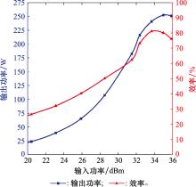
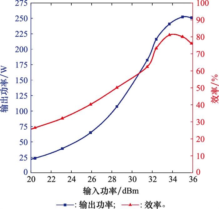
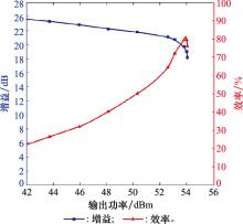
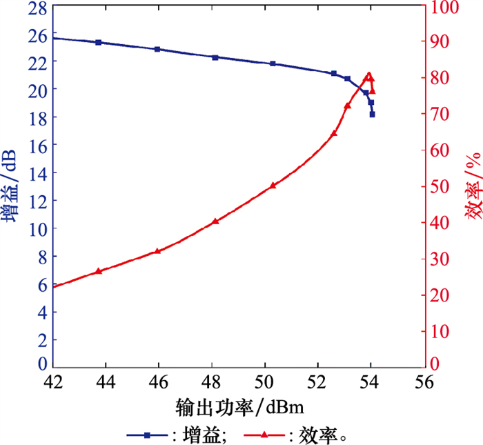
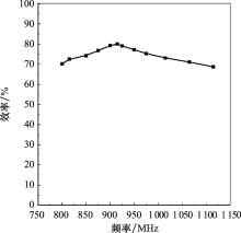
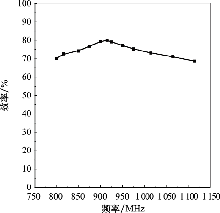
| 1 |
ZISSIS G , KITSINELIS S . State of art on the science and technology of electrical light sources: from the past to the future[J]. Journal of Physics D: Applied Physics, 2009, 42 (17): 16.
|
| 2 |
GODYAK A V . Bright idea: radio-frequency light sources[J]. IEEE Industry Applications Magazine, 2002, 8 (3): 42- 49.
doi: 10.1109/2943.999612
|
| 3 |
SATOSHI H , NICK S . RF power semiconductor generator application in heating and energy utilization[M]. Singapore: Springer Nature Singapore Pte Ltd, 2020.
|
| 4 |
ROBERT K , CHERNG S C , GEORGES Z , et al. Handbook of advanced lighting technology[M]. Switzerland: Springer International Publishing, 2017.
|
| 5 |
黄桃, 卢辉, 王茂碧, 等. 微波等离子体光源研究[J]. 真空电子技术, 2013 (6): 73- 75.
|
|
HUANG T , LU H , WANG M B , et al. Research on light emitting plasma[J]. Vacuum Electronics, 2013 (6): 73- 75.
|
| 6 |
GILLIARD R P , DEVINCENTIS M , HAFIDI A , et al. Operation of the LiFi light emitting plasma in resonant cavity[J]. IEEE Trans. on Plasma Science, 2011, 39 (4): 1026- 1033.
doi: 10.1109/TPS.2011.2113358
|
| 7 |
贾华, 单家芳, 刘甫坤, 等. 射频等离子体光源高效固态功率源的设计[J]. 核聚变与等离子体物理, 2021, 41 (1): 91- 96.
|
|
JIA H , SHAN J F , LIU F K , et al. Design of high efficiency solid state power source for radiofrequency plasma light[J]. Nuclear Fusion and Plasma Physics, 2021, 41 (1): 91- 96.
|
| 8 |
蒂莫西·J·布洛克特, 戴维·P·施梅尔策, 迈赫兰·马特路比安, 等. 等离子体灯的螺旋结构及方法[P]. 中国:
|
|
CN201080024516. X, 2012.05.16. TIMOTHY J B, DAVID P S, MEHUL M, et al. Helical structure and method of plasma lamp[P]. China: CN201080024516. X, 2012.05.16.
|
| 9 |
XU M Y , JIA H , HUAN W D , et al. A startup control method for plasma lamps by using fractional-n phase-locked loop microwave driver[J]. Electronics, 2022, 11 (16): 2576.
doi: 10.3390/electronics11162576
|
| 10 |
JIA H , XU M Y , HUAN W D , et al. Improving luminous efficacy of ceramic resonator plasma lamps by using microwave pulse modulation[J]. IEEE Trans. on Plasma Science, 2022, 50 (9): 2932- 2940.
doi: 10.1109/TPS.2022.3195346
|
| 11 |
DEVINCENTIS M , HOLLINGSWORTH G , GILLIARD R . Long life solid-state RF powered light sources for projection display and general lighting applications[J]. IEEE MTT-S International Microwave Symposium Digest, 2008, 1497- 1500.
|
| 12 |
史强, 要志宏, 蒙燕强, 等. L波段1500W GaN功率放大器[J]. 半导体技术, 2023, 48 (3): 218- 223.
|
|
SHI Q , YAO Z H , MENG Y Q , et al. L-band 1500 W GaN power amplifier[J]. Semiconductor Technology, 2023, 48 (3): 218- 223.
|
| 13 |
王帅, 段亚朋, 毋皓, 等. 高效率双频连续F类功率放大器的设计[J]. 电子元件与材料, 2023, 42 (1): 88- 95.
|
|
WANG S , DUAN Y P , WU H , et al. Design of high efficiency dual-band continuous Class F power amplifier[J]. Electronic Components and Materials, 2023, 42 (1): 88- 95.
|
| 14 |
孙园成. 基于GaN的新型F类功率放大器的研究与设计[D]. 成都: 电子科技大学, 2021.
|
|
SUN Y C. Research and design of novel Class F power amplifiers based on GaN[D]. Chengdu: University of Electronic Science and Technology of China, 2021.
|
| 15 |
郑晓玲. F类功率放大器研究[D]. 杭州: 杭州电子科技大学, 2019.
|
|
ZHENG X L. Research on Class F power amplifier[D]. Hangzhou: Hangzhou Dianzi University, 2019.
|
| 16 |
MERVE A , FIRAT K , SEDAT K . Design of a Class F power amplifier with GaN device model and reflection data[J]. IEEE Journal of Research, 2023, 69 (2): 1117- 1123.
|
| 17 |
ZHAO H Y , ZHANG D . Wideband Class F power amplifier design based on harmonic control analysis and bandwidth expansion structure[J]. Microwave and Optical Technology Letters, 2022, 65 (1): 109- 114.
|
| 18 |
JIA M S , CHENG Z Q , SHI Y R , et al. Wideband high-efficiency extended continuous Class F power amplifier using a new wideband bandstop network[J]. Microwave and Optical Technology Letters, 2022, 64 (11): 1965- 1971.
|
| 19 |
XIA J , BIAN C X , KONG W , et al. Optimization design of fragment-type filtering matching network for continuous inverse Class F power amplifier[J]. IEICE Electronics Express, 2022, 19 (14): 11- 13.
|
| 20 |
亓孝博. 微波功率放大器的效率提升及小型化研究[D]. 成都: 电子科技大学, 2020.
|
|
QI X B. Research on efficiency improvement and miniaturization of microwave power amplifier[D]. Chengdu: University of Electronic Science and Technology of China, 2020.
|
| 21 |
YANG F , YU H X , LI J , et al. Substrate integrated waveguide based Class F power amplifier[J]. Electronics Letters, 2021, 58 (1): 22- 24.
|
| 22 |
SEPEHR Z , MOHSEN H , MARIAN K , et al. A novel design methodology for extended continuous Class F power amplifiers in wireless applications[J]. Wireless Networks, 2021, 27 (6): 3947- 3968.
|
| 23 |
南敬昌, 张鹏俊, 高明明, 等. 基于GaN器件的平衡式逆F类功率放大器的研究与设计[J]. 重庆邮电大学学报(自然科学版), 2019, 31 (1): 80- 88.
|
|
NAN J C , ZHANG P J , GAO M M , et al. Research and design of the balanced inverse Class F power amplifier based on GaN devices[J]. Journal of Chongqing University of Posts and Telecommunications(Natural Science Edition), 2019, 31 (1): 80- 88.
|
| 24 |
SINDER D M . Nonlinear analysis and design of overdriven Class B power amplifiers[J]. IEEE Trans. on Microwave Theory and Techniques, 1967, 63 (8): 2567- 2575.
|
| 25 |
丁瑶. 高效率射频功率放大器的研究[D]. 合肥: 中国科学技术大学, 2013.
|
|
DING Y. Research on high efficiency radio frequency power amplifiers[D]. Hefei: University of Science and Technology of China, 2013.
|
| 26 |
李玉龙. F类/逆F类功率放大器研究与设计[D]. 桂林: 广西师范大学, 2016.
|
|
LI Y L. F Class/Inverse F Class power amplifier research and design[D]. Guilin: Guangxi Normal University, 2016.
|
| 27 |
GREBENNIKOV A . Load network design technique for Class F and inverse Class F power amplifiers[J]. High Frequency Electronics, 2011, 11 (5): 22- 32.
|
| 28 |
POSADAS G V , MARTIN J L J , CERRADA P A , et al. Stability, mounting, and measurement considerations for high-power GaN MMIC amplifier[J]. Sensors, 2023, 23 (23): 234- 236.
|
| 29 |
WONSHIL K , HYUNCHUL K . An efficient plasma lighting system with a 300W GaN power amplifier using band-limited pulsed RF signal[J]. IEICE Transactions on Electronics, 2017, E100.C (10): 934- 937.
|
| 30 |
钟世昌, 陈堂胜, 殷晓星, 等. 基于大信号模型的L波段400W高效Ga N功率放大器设计[J]. 电子学报, 2020, 48 (2): 398- 402.
|
|
ZHONG S C , CHEN T S , YIN X X , et al. GaN L-Band 400W power amplifier design using large signal model[J]. Acta Electronica Sinica, 2020, 48 (2): 398- 402.
|